|
The objective of this lab is to introduce you to simulating systems using System C and viewing the results using a waveform viewer (gtkwave)
The second systems coursework uses System C, so this lab will help you with this coursework.
System C is essentially a hardware description language. In reality it is a library of methods based on C++, an object-oriented enhancement of the C programming language.
This course does not teach you System C, nor are you advised to learn it by yourselves at this stage. We are merely using it as a simulation engine because it can effectively model concurrent operations, closely mimicking the operation of real hardware. The code that you are required to write will be plain C and will not use any of the System C features. The provided code will obviously use System C features but you are not required to learn how it works. What you need to understand is how simple computer hardware works, not the details of how to model it using System C.
For this lab you will simulate three small circuits to get familiar with running simulations and viewing the results in a waveform viewer called gtkwave.
Copy the following files into a directory/folder in your disk space.
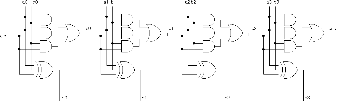
The above files represent a 4-bit carry-ripple adder just like the one shown below. The gates at the bottom of the figure which drive the sum outputs are 3-input XOR gates: the output is 1 when any one or all three inputs are 1, 0 otherwise.
Open a terminal, change to the directory where you copied the above files and type make. This will compile the System C code and produce an executable called cra. When you run it, it creates a file called waves.vcd. This file contains the waveform: a description of all the circuit's signals (inputs, outputs and internal wires) and how they change in time. To view the waveform, type gtkwave waves.vcd This opens up the gtkwave application. On the left hand side, you will see "SystemC" inside a text box. Click on it and you will get a list of signal names in the box below. You can now select any signals and click on the Append button below to display them in the large black area to the right. To see the full waveform click on the second button on the top row of the Zoom group of buttons. This will zoom out as far as possible so you can see the entire simulation time and all the signal changes. Now you can zoom in to look at the details. If you click on the Waves area, you get a vertical red marker. This will show you the value of each signal at that time at the left of the waveform.
Explore the various buttons and options of gtkwave. One feature you will find useful is to change the data format options (available under the Edit menu). You can change the data format into binary, hexadecimal, decimal, etc. You can change the format of each signal individually.
Now clear up all the signals from the waves box and let's explore how the adder works. First find the circuit inputs a3-a0, b3-b0 and cin and add their waves. Zoom out fully to see which numbers are being added. Now add the waveform of the outputs s3-s0 and the carry out cout. Finally add the intermediate signals c0-c2.
The inputs change at times 0ns, 30ns and 60ns. Note that the waveform ends abruptly when the last change happens. Be careful to see the very last output values, which should be (s3-s0 = 0101)
Verify that the adder works correctly for the provided input values. Notice the case where the adder overflows and gives a sum of 0 for the second set of inputs.
Now let's focus on the propagation delays. Notice that from the time the inputs change, it takes a while for the outputs to change to the correct values. This time depends on the gate delays and the actual values of the inputs. In some cases the outputs may change a number of times before they stabilise to the correct values. You can see this happening for the second set of inputs. Look at the intermediate carry signals to see how they change and notice the ripple effect when adding 0111 and 0001.
If you feel a little adventurous, try changing driver.cpp to provide some other inputs to the adder. All you have to do is modify the binary values inside the double quotes. The first bit after the 'b' is the one that gets assigned to a3 (or b3) and the last is the one that gets assigned to a0 (b0). You have to re-compile (make), re-run (./car) and load the new waves into gtkwave to see the results.
Copy the following files into a directory/folder in your disk space.
The above files represent a 4-bit shift register just like the one shown below.
The inputs to the circuit are the clock signal (clk) and a 1-bit input, din.
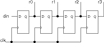
Compile (make), run (./shr) and start the waveform viewer (gtkwave waves.vcd). Add all signals to the waveform box. You will probably find it more useful to change the data format of r into binary. Click on r (next to the waveform box) to select it and expand it (under Edit) into separate bits.
Observe how the shift register works. Initially all D flip-flops (r0-r3) contain 0s. The first input (din) is 0 so when the first rising clock edge arrives, nothing changes in r0-r3. Before the following rising clock edge arrives, input din is set to 1. This 1 is propagated into the first flip-flop (r0 = 1 shortly after the following rising clock edge). It then continues its way through the shift register, while new data enters from the left. Notice how many cycles it takes for a new input in din to propagate to the end of the shift register.
Copy the following files into a directory/folder in your disk space.
The above files model the implementation of the vending machine FSM described at the end of chapter 5 of the course notes. The inputs to the circuit are the clock signal (clk), a signal representing that a 10p coin has been inserted ten and a signal for a 20p coin twenty.
Compile, run and open the results in gtkwave. Observe the operation of the circuit. In particular notice the timing of the output signal z and the state transitions. As specified in the notes, z becomes 1 whenever the state s3 (encoded as 11 in binary) is reached. State transition follows the FSM diagram and the state encoding follows that of the table.
Convince yourself that you understand the timing issues of the FSM: when, in relation to the clock edges, are the inputs applied, when do they change the state of the machine, and when the output signal takes on its new value.
|
Informatics Forum, 10 Crichton Street, Edinburgh, EH8 9AB, Scotland, UK
Tel: +44 131 651 5661, Fax: +44 131 651 1426, E-mail: school-office@inf.ed.ac.uk Please contact our webadmin with any comments or corrections. Logging and Cookies Unless explicitly stated otherwise, all material is copyright © The University of Edinburgh |